CMOS LOGIC
The basic building blocks
in CMOS logic circuits are MOS transistors.
1. CMOS Logic Levels
Abstract logic elements
process binary digits, 0 and 1. But the real logic circuits process electrical
signals such as voltage levels. In any logic circuit, there is a range of
voltages (or other circuit conditions) that is interpreted as logic 0, and
another, nonoverlapping range that is interpreted as logic 1.
A typical CMOS logic
circuit operates from a 5-volt power supply. Such a circuit may interpret any
voltage in the range 0–1.5 V as logic 0 (LOW), and in the range 3.5–5.0 V as a
logic 1 (HIGH) as shown in fig.1. Voltages in the intermediate range are not
expected to occur except during signal transitions, and yield undefined logic
values (i.e., a circuit may interpret them as either 0 or 1). CMOS circuits
using other power supply voltages, such as 3.3 or 2.7 volts, partition the voltage
range similarly.

2. MOS Transistors
A MOS transistor can be
modeled as a 3-terminal device that acts like a voltage controlled resistance,
as shown in fig.2. An input voltage applied to one terminal controls the
resistance between the remaining two terminals. In digital logic applications,
a MOS transistor is operated so its resistance is always either very high (and
the transistor is “off”) or very low (and the transistor is “on”).

Types
of MOS transistors
(a) n-channel MOS
(b) p-channel MOS
The
names refer to the type of semiconductor material used for the
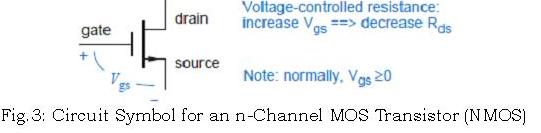
resistance-controlled terminals. The circuit symbol for an n-channel MOS
(NMOS) transistor is shown in Fig.3. The terminals are called gate,
source, and drain. From the orientation of the circuit symbol, the
drain is normally at a higher voltage than the source. The voltage from gate to source (Vgs) in an NMOS
transistor is normally zero or positive. If Vgs = 0, then the resistance
from drain to source (Rds) is very high, on the order of a megohm (106
ohms) or more. As we increase Vgs (i.e., increase the voltage on the
gate), Rds decreases to a very low value, 10 ohms or less in some
devices.
The circuit symbol for a p-channel
MOS (PMOS) transistor is shown in Fig.4. Operation is analogous to that of
an NMOS transistor, except that the source is normally at a higher voltage than
the drain, and Vgs is normally zero or negative. If Vgs is zero,
then the resistance from source to drain (Rds) is very high. As we
algebraically decrease Vgs (i.e., decrease the voltage on the
gate), Rds decreases to a very low value.

The gate of a MOS transistor has very
high impedance i.e., the gate is separated from the source and the drain by an
insulating material with a very high resistance. However, the gate voltage
creates an electric field that enhances or retards the flow of current between
source and drain, which is the “field effect” in the “MOSFET” name. Regardless
of gate voltage, almost no current flows from the gate to source, or from the
gate to drain for that matter. The resistance between the gate and the other terminals of the device is extremely high, around a
mega ohm. The small amount of current that flows across this resistance is very
small, i.e., <1µA called as leakage
current.
The MOS transistor symbol
itself shows that there is no connection between the gate and the other two
terminals of the device. However, the gate of a MOS transistor is capacitively
coupled to the source and drain. In high-speed circuits, the power needed to
charge and discharge this capacitance on each input-signal transition accounts
for a nontrivial portion of a circuit’s power consumption.
3. Basic CMOS Inverter Circuit
NMOS and PMOS transistors
are used together in a complementary way to form CMOS logic. The
simplest CMOS circuit, a logic inverter, requires only one of each type of
transistor, connected as shown in Fig.5 (a). The power supply voltage, VDD,
ranges from 2V to 6V, and is most often set at 5.0 V for compatibility with TTL
circuits.

Ideally, the functional
behavior of the CMOS inverter circuit can be characterized by just two cases
tabulated in Fig.5 (b).
1.
When VIN is 0.0 V(L), the
bottom, n-channel transistor Q1 is off, since its Vgs is 0, but the top, p-channel transistor Q2
is on, since its Vgs is a large negative value (-5.0 V). Hence Q2 presents
only a small resistance between the power supply terminal (VDD, +5.0 V) and the output
terminal (VOUT), and the output voltage is 5.0 V.
2.
When
VIN is 5.0 V (H), Q1 is
on, since its Vgs is a large positive value (+5.0 V), but Q2 is
off, since its Vgs is 0. Thus, Q1 presents a small resistance
between the output terminal and ground, and the output voltage is 0V.

As shown in Fig.6 (a), the n-channel
(bottom) transistor is modeled by a normally-open switch and the p-channel
(top) transistor by a normally-closed switch. Applying a HIGH voltage changes each switch
to the opposite of its normal state, as shown in Fig.6 (b).

The Fig.7 shows the different symbols
used for the p- and n-channel transistors to reflect their
logical behavior. The n-channel transistor (Q1) is switched “on,”
and current flows between source and drain, when a HIGH voltage is applied to its gate. The p-channel
transistor (Q2) has the opposite behavior, i.e., it is “on” when a LOW
voltage is applied; the
inversion bubble on its gate indicates this inverting behavior.
4.
CMOS NAND and NOR Gates
Both NAND and NOR gates can be constructed
using CMOS. A k-input gate uses k p-channel and k n-channel
transistors. Fig.8 shows a 2-input CMOS NAND
gate, where if either input
is LOW, the output Z has a low-impedance connection to VDD
through the corresponding “on” p-channel transistor, and the path to
ground is blocked by the corresponding “off” n-channel transistor. If
both inputs are HIGH, the path to VDD is blocked, and Z has a low-impedance
connection to ground. Fig.9 shows the switch model for the NAND gate’s operation.


Fig.10 shows a CMOS 2-input
NOR gate. If both inputs are LOW, the output Z
has a low-impedance
connection to VDD through the “on” p-channel transistors, and the
path to ground is blocked by the “off” n-channel transistors. If either
input is HIGH, the path to VDD is blocked, and Z has a low-impedance
connection to ground.

5. Fan-In
The number of inputs that a
gate can have in a particular logic family is called the logic family’s fan-in.
CMOS gates with more than two inputs can be obtained by extending
series-parallel designs on Figures 8 and 10 in the obvious manner.

Consider a 3-input CMOS NAND gate as shown in Fig.11. In
principle, we can design a CMOS NAND
or NOR gate with a very large
number of inputs. But practically, the additive “on” resistance of series
transistors limits the fan-in of CMOS gates, typically to 4 for NOR gates and 6 for NAND gates.
As the number of inputs is
increased, CMOS gate designers may compensate by increasing the size of the
series transistors to reduce their resistance and the corresponding switching
delay. But at some point this becomes inefficient or impractical. Gates with a
large number of inputs can be made faster and smaller by cascading gates with
fewer inputs.

Eg. Consider the logical
structure of an 8-input CMOS NAND gate as shown in Fig.12, the total delay through
a 4-input NAND, a 2-input NOR, and an inverter is typically less than the delay of a one-level
8-input NAND circuit.
6. Noninverting Gates
In CMOS and most other
logic families, the simplest gates are inverters, and the next simplest are NAND gates and NOR gates. A logical inversion
comes “for free,” and it typically is not possible to design a noninverting
gate with a smaller number of transistors than an inverting one.


CMOS noninverting buffers
and AND and OR gates are obtained by connecting an inverter to the output of the
corresponding inverting gate. Thus, Fig.13 shows a noninverting buffer and Fig.14
shows an AND gate.
7. CMOS AND-OR-INVERT and
OR-AND-INVERT Gates
CMOS circuits can perform
two levels of logic with just a single “level” of transistors. A two-wide,
two-input CMOS AND-OR-INVERT (AOI) gate and its function table are shown in fig.15 (a) and (b). The corresponding logic diagram
for this function using AND and NOR gates is shown in Fig.16.


Transistors can be added to
or removed from this circuit to obtain an AOI
function with a different
number of ANDs or a different number of inputs per AND.
The contents of each of the
Q1–Q8 columns in Fig.15(b) depends only on the input signal
connected to the corresponding transistor’s gate. The last column is
constructed by examining each input combination and determining whether Z is connected to VDD
or ground by “on” transistors for that input combination. Z is never connected to both
VDD and ground for any input combination; in such a case the output would
be a non-logic value some- where
between LOW and
HIGH,
and the output structure would consume excessive power due to the low-impedance
connection between VDD and ground.
A circuit can also be designed to
perform an OR-AND-INVERT function.
A two-wide, two-input CMOS OR-AND-INVERT (OAI) gate and its function
table is as shown in fig.17 (a) and (b), the values in each column are
determined just as we did for the CMOS AOI gate. The logic diagram for the OAI function using OR and NAND gates is shown in Fig.18.


The speed and other electrical
characteristics of a CMOS AOI or OAI gate
are quite comparable to those of a single CMOS NAND
or NOR gate, i.e., they can perform two levels of logic (AND-OR or OR-AND) with just one level of delay. Most digital designers use AOI gates in their discrete designs. Also,
CMOS VLSI devices often use these gates internally, since many HDL synthesis
tools can automatically convert AND/OR logic into AOI gates when appropriate.
This is very useful and informative, Thanks for sharing. Semicon Technologies Pvt Ltd|VLSI Training Institute in Bangalore
ReplyDeleteI really liked your Information. Keep up the good work.
ReplyDeletelogic chips