CHAPTER-1
Introduction to RF Design
Radio-frequency (RF)
electronics differ from other electronics because the higher frequency circuit
operation is hard to understand due to
1.
Stray
capacitance is the capacitance that exists between conductors of the circuit,
between conductors or components and ground, or between components. (VHF TV
Tuners)
2.
Stray
inductance is the normal inductance of the conductors that connect components,
as well as internal component inductances.
3.
Skin
effect refers to the fact that ac flows only
on the outside portion of the conductor, while dc flows through the entire
conductor. As frequency increases, skin effect produces a smaller zone of
conduction and a correspondingly higher value of ac resistance compared with dc
resistance.
4.
The
signals at Radio Frequencies easily radiate both from the circuit and within
the circuit.
5.
Coupling
effects between elements of the circuit, between the circuit and its
environment, and from the environment to the circuit become a lot more critical
at RF. Interference and other strange effects are found at RF that are missing
in dc circuits and are negligible in most low frequency ac circuits.
The electromagnetic spectrum
When an RF electrical
signal radiates, it becomes an electromagnetic wave that includes not only
radio signals, but also infrared, visible light, ultraviolet light, X-rays,
gamma rays, and others.
The electromagnetic
spectrum is broken into bands for the sake of convenience and identification.
The extremely low frequency (ELF) range includes ac power-line frequencies as
well as other low frequencies in the 25- to 100-hertz (Hz) region. The U.S.
Navy uses these frequencies for submarine communications.

Fig.1:
The Electromagnetic Spectrum from VHF to X-ray. The RF region covers from less
than 100KHz to 300GHz.
The amplitude-modulated
(AM) broadcast band (540 to 1630 kHz) spans portions of the LF and MF bands.
The high-frequency (HF)
region, also called the shortwave bands (SW), runs from 3 to 30 MHz. The
VHF band starts at 30 MHz and runs to 300 MHz. This region includes the
frequency-modulated (FM) broadcast band, public utilities, some television stations,
aviation, and amateur radio bands.
The ultrahigh frequencies
(UHF) run from 300 to 900 MHz and include many of the same services as VHF.
The microwave region
begins above the UHF region, at 900 or 1000 MHz, depending on source authority.
Microwaves almost become
a separate topic in the study of RF circuits because at these frequencies the
wavelength approximates the physical size of ordinary electronic components.
Thus, components behave differently at microwave frequencies than they do at
lower frequencies.
At microwave frequencies,
a 0.5-W metal film resistor, for example, looks like a complex RLC network with
distributed L and C values
and a surprisingly different R value.
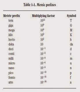
Units in RF Design
In accordance with
standard engineering and scientific practice, all units in this book will be in
either the CGS (centimeter-gram-second) or MKS (meterkilogram- second) system
unless otherwise specified.


Wavelength and frequency
For all wave forms, the
velocity, wavelength, and frequency are related so that the product of
frequency and wavelength is equal to the velocity. For radiowaves, this
relationship can be expressed in the following form:
eq1
Where λ – Wavelength in m, f –
Frequency in Hz, ε – Dielectric Constant of the
Propagation Medium, c – Velocity of Light.
The dielectric constant (ε
) is a property of the medium in which the wave propagates.
The value of is defined
as 1.000 for a perfect vacuum and very nearly 1.0 for dry air (typically
1.006). In most practical applications, the value of ε in dry air is taken to
be 1.000. For media other than air or vacuum, however, the velocity of propagation
is slower and the value of ε relative to a vacuum is higher. Eg.:
Teflon can be made with values from about 2 to 11. eq2
Microwave letter bands
During World War II, the
U.S. military began using microwaves in radar and other applications. For
security reasons, alphabetic letter designations were adopted for each band in
the microwave region. T1 T2 T3


Skin effect
Reasons for ordinary
lumped constant electronic components to not work well at microwave frequencies
are
1.
Component
size and lead lengths approximate microwave wavelengths.
2.
The
distributed values of inductance and capacitance become significant at these
frequencies.
3.
The
phenomenon of skin effect. While dc current flows in the entire cross section
of the conductor, ac flows in a narrow band near the surface. Current density
falls off exponentially from the surface of the conductor toward the center. At
the critical depth (δ, also called the depth of penetration), the
current density is 1/e = 1/2.718= 0.368 of the surface current density.

Fig.2: In ac Circuits, the current
flows only in the outer region of the conductor.
This effect is frequency-sensitive and it becomes a serious consideration at
higher RF frequencies.
eq3
eq3

Where δ
– Critical Depth, f – Frequency in Hz, μ – Permeability in H/m, σ – Conductivity in mhos/m.
INTRODUCTION TO RF AND WIRELESS
TECHNOLOGY
Phone sets with increasingly higher performance require reducing
power consumption and cost by nearly 30% every year. An “omnipotent” wireless
terminal can handle voice, data and video as well as computing power – Personal
Communication Services (PCS).
COMPLEXITY COMPARISON


Fig.3: FM Transmitter Fig.4: FM Receiver
In FM Transmitter, Q1 operates as both an Oscillator and a
frequency modulator.i.e., the audio signal produced by the microphone varies
the bias voltage across the varactor diode D1, thereby modulating the frequency
of oscillation. In FM Receiver, Q1 operates as both an Oscillator and a demodulator.

Fig.5: RF Section of a Cell Phone
DESIGN BOTTLENECK
Phone contains small fraction operating in RF Range and the
rest performing Low-Frequency “Baseband” analog and digital signal Processing.


Fig.6: RF and Baseband processing Fig.7: Disciplines required in RF
in a Transceiver. Design
RF
DESIGN HEXAGON
RF Circuits must process analog signals
with a wide dynamic range at high frequencies. RF Circuits cannot be
manufactured using IC Technology as it requires external components such as
inductors that are difficult to fabricate.

Fig.8: RF
Design Hexagon
DESIGN
TOOLS
Computer Aided Analysis and Synthesis Tools
are still in developing Stage due to the following issues.
1. As Nonlinearity, Time Variance and Noise in RF Circuits usually
require studying the spectrum of signals, but the standard ac analysis in SPICE
uses only Linear, Time Invariant models. Hence circuits are simulated in time domain
and transformed to frequency domain to obtain spectrum, but time domain simulation
has to run for a long period to resolve closely spaced frequency components. Also
spectral averaging techniques may be necessary if random noise is used in time domain
analysis.
2. The external components like surface acoustic wave (SAW) filters,
used in both transmit and receive paths exhibit input and output impedances that
can be characterized by only S-Parameters (essentially a table of numbers), cannot
be modeled by typical devices in SPICE. Hence modeling such circuits with RLC networks
provides a first order approximation and it may not predict effects such as instability
and impedance mismatch.
APPLICATIONS
1.
Pagers
2.
Cell
Phones
3.
WLANs
– use frequency bands around 900MHz and 2.4GHz. WLAN Tranceivers can provide mobile
connectivity in offices, hospitals, factories, etc instead of using cumbersome wired
networks. Prominent features are Portability and reconfigurability.
4.
GPS
- To obtain one’s location and direction. Operates
in 1.5GHz for automobile industry as low-cost hand held products.
5.
RFIDs
– RF Identification systems are small low cost tags attached to objects or persons
to track their position. Luggabe bags in airports to troops in military operations.
Advantages – Low power consumption, long tag’s lifetime, single small battery. 900MHZ
to 2.4GHz.
6.
Home
Satellite Network – operate in 10 GHz, require additional dish antenna and a receiver
to a television set.
ANALOG AND DIGITAL SYSTEMS


Fig.9: Block Diagram of a generic analog
RF system Transmitter and Receiver.
In analog architecture, in the transmit path, the signal generated
by the microphone modulates a HF carrier and the resultant signal is amplified and
buffered to drive the antenna. In the receive path, the signal is amplified by a
LNA, the spectrum is translated to a LF by a downconverter (mixer) to facilitate
subsequent demodulation, and the demodulated output is amplified to drive the speaker.

Fig.10: Block Diagram of a generic digital
RF system with transmitter and receiver.
In digital architecture, Voice Compression is used to reduce
bit rate and Bandwidth. Coding and Interleaving to detect and minimize errors. Pulse
Shaping is used as rectangular pulses are usually not optimum for modulation.
The performance of transceivers can be quantified in terms of
maximum distance across which they operate while providing satisfactory reception
which is determined by both the power delivered to the antenna and the sensitivity
of the receiver due to noise of LNA.
Practically, many different transceivers operate simultaneously,
often in close proximity, thereby interfering with each other. Also the communication
medium is quite complex: reflections from buildings and other obstacles can result
in destructive interference at a given point, suppressing the received signal strength
to undetectable levels. Hence in such an environment, signal processing in the digital
transmitter achieves higher performance than that of the analog system.
In RF domain, the spectrum
is not centered around zero frequency. The Modulator, Power Amplifier, Low Noise
Amplifier and the Downconverter operate in RF range.
CHOICE OF TECHNOLOGY
Performance, Cost and Time to Market are three critical factors
that influence the choice of technology in competitive RF industry.
Issues such as level of integration, form factor and prior experience
play an important role in the decisions made by the designers.
Technologies used in RF:
1.
GaAs
2.
Silicon
Bipolar
3.
BiCMOS
Technology
GaAs Field effect and heterojunction devices are low yield, high
power and high cost option used Power Amplifies and front-end switches.
GaAs processes offer useful features like higher (breakdown voltage)(cutoff
Frequency) product, semi-insulating substrate, and high-quality inductors and capacitors.
Silicon (Bipolar) devices in a VLSI Technology can potentially
provid both higher levels of integration and lower overall cost, as demonstrated
in complex circuits such as frequency synthesizers.
CMOS Technology devices have high transit frequencies, e.g.,
tens of gigahertz in the 0.35μm
generation. CMOS technology resolves a number of practical issues like substrate
coupling of signals that differ in amplitude by 100dB, parameter variation with
temperature and process, and device modeling for RF operation.